Three product lines. One measurement platform.
Vision inspection and metrology for PCB micro-holes, post-dicing edge defects, and semiconductor test-pin arrays. Choose a product direction and prepare representative samples; Insightek responds with a feasibility conclusion and a demo report — no need to decide on equipment up front.
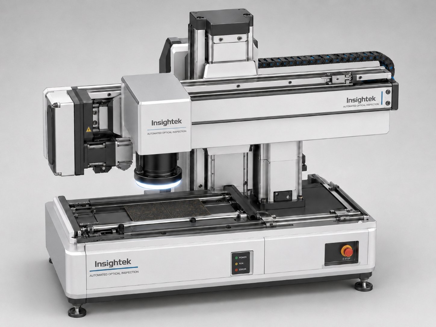
PCB Micro-Hole Measurement & Inspection
Turn every hole into traceable measurement data and a verdict.
With hole counts from hundreds of thousands to tens of millions, sampling is bound to miss local drift. Large-field single-shot imaging plus massively parallel per-hole computation turn every hole into traceable measurement data and a verdict.
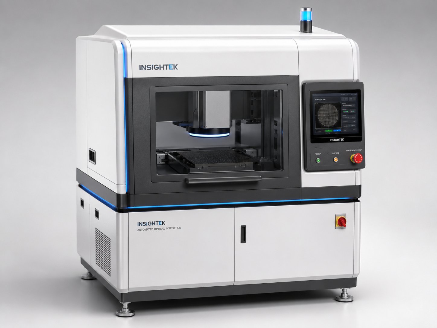
Post-Dicing Inspection & Edge Quantification
Intercept bad dies at the post-dicing stage — before they consume downstream packaging materials, bonding hours, and whole-unit test cost.
Diced edges and sidewalls are the high-risk zone entering advanced packaging. Full-wafer inspection at the post-dicing stage detects edge anomalies, separates real defects from saw marks, and outputs position, size, and class — so high-risk dies are caught before they move on.
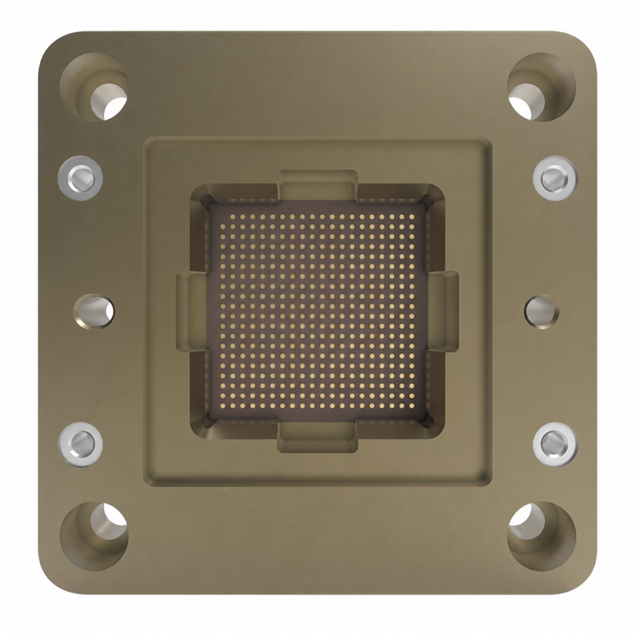
Test-Pin Inspection & Lifecycle Control
Turn carrier status from "visually checked" into "quantitatively confirmed."
Test carriers keep evolving toward higher bandwidth, finer pitch, and higher pin counts — and pin consistency directly bounds yield and test stability. Insightek quantifies pin height, coplanarity, positional offset, and surface condition pin by pin, across high-density test-pin arrays and test sockets.
Start with a sample validation.
| Product direction | Targets | Key outputs | Confirm before adoption |
|---|---|---|---|
| PCB micro-holes | Micro-holes & blind vias on PCB, HDI, IC substrates | Diameter, roundness, position, concentricity, burrs/nicks, full-panel quality map | Field size, hole count, target accuracy, takt, surface condition |
| Post-dicing | Wafer / die dicing edges, sidewalls, surfaces | Cracks, chipping, notches, particles, surface anomalies with defect position & size | Defect samples, optics, re-judgment rules, stitching range, takt |
| Semiconductor test pins | Test pins, probe heads, package-test socket arrays | Pin height, coplanarity, offset, contamination/wear, repair re-inspection reports | Array density, fixturing, measurement items, maintenance flow, acceptance criteria |
Phased adoption, controlled risk.
Three delivery tiers, starting from sample validation — each step with clear deliverables and no one-shot bet.
Software Solution
Models + platform + interfaces
Integrated HW/SW Unit
Algorithms + AI compute box + industrial integration
Standard Equipment
Full machine + AI inspection system + data loop
Not sure which direction fits?
Send representative samples — good parts plus known anomalies — and we will return a feasibility conclusion and a demo report.