PCB Micro-Hole Measurement & Inspection
Turn every hole into traceable measurement data and a verdict.
With hole counts from hundreds of thousands to tens of millions, sampling is bound to miss local drift. Large-field single-shot imaging plus massively parallel per-hole computation turn every hole into traceable measurement data and a verdict.
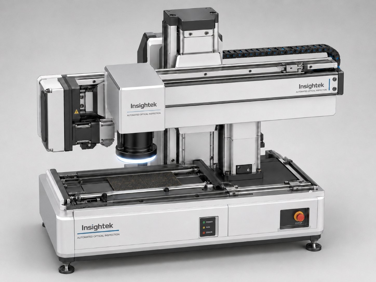
Three advantages that survive the procurement conversation.
One owner closes the loop
Models, software, AI compute, and equipment are all developed in-house — so accuracy, speed, and false-call issues never bounce between vendors.
Large field, micron resolution, high speed
High-speed micron-level stitching plus hardware-accelerated compute let 1000 mm fields coexist with micron-level metrology, and throughput scales with compute.
Real-vs-false verdicts you can verify
Dedicated models trained on your samples separate real defects from false calls, with overkill and escapes accepted against a jointly agreed sample set.
When holes number in the millions, sampling can’t keep up.
High-density micro-hole arrays share the same failure mode: huge target counts, tiny defects, and gradual, uneven degradation that low-coverage sampling and manual inspection are poor at catching.
Sampling can’t cover millions of holes.
With hole counts from hundreds of thousands to tens of millions, low-coverage sampling is bound to miss local drift — the few holes you check say nothing about the ones you don’t.
Local process drift hides between samples.
Dense arrays degrade gradually and unevenly. A sampling plan that passes can still let a drifting region of the panel slip through unnoticed.
Escapes get more expensive at every step.
As a general industry rule of thumb, a defect fixed at your own step costs 1, the next step 10, and at the customer 100. The actual magnitudes are estimated jointly with your process costs, but the direction never changes.
Burr and nick calls stay subjective.
Ambiguous hole-wall burrs and edge nicks lead to inconsistent manual re-judgment, adding overkill and disagreement between inspectors and shifts.
Five steps, each with a deliverable you keep.
From sample validation to line-side inspection, every step ends with something concrete in your hands — so you decide the next step on evidence, not on a promise.
- 01
Sample & process review
You provide representative samples and target metrics; Insightek assesses feasibility. You receive a feasibility conclusion.
- 02
Imaging & algorithm validation
Insightek selects the optics and validates the metrology and detection models on your samples. You receive a detection and metrology demo report.
- 03
Inspection items & thresholds
Verdict thresholds and acceptance criteria are agreed on a shared sample set. You receive a verdict scheme plus acceptance criteria.
- 04
Line-side integration & data output
Interfaces are hooked up, pilot runs confirm takt, and data output is verified. You receive an integration validation report.
- 05
Acceptance, replication & iteration
Formal acceptance, multi-line replication, and model iteration follow. You receive an acceptance report and a maintenance plan.
To prepare: representative samples (good / defect / borderline plus re-judgment results), target metrics (accuracy, escape / overkill, takt), process details, interface formats (PLC / MES / SPC / SECS-GEM or report formats), and acceptance rules.
What the system measures and judges on every hole.
Per-hole diameters, center spacing, and verdicts — values computed in pixels and converted to μm via calibrated pixel size, then rolled up across the whole panel.
Diameter & roundness
Per-hole geometric metrology across the full array, not a sampled subset.
- Diameter and roundness measured for every hole
- Values computed in pixels and converted to μm via calibrated pixel size
- Per-hole results feed process tuning and anomaly tracing
Position & concentricity
Panel and layer registration checked hole by hole.
- Hole position and center spacing measured across the panel
- Concentricity evaluated against panel and layer registration
- Surfaces registration and alignment drift for anomaly tracing
Hole-wall burrs & edge nicks
AI real-vs-false discrimination on the calls that are hardest to make consistently.
- Hole detection fused with geometric verdict models
- Real burrs and nicks separated from false calls
- Less manual re-judgment, more consistent verdicts
Full-panel hole quality map
Every hole rolled up into one map that pinpoints local process drift.
- Panel-wide quality map built from per-hole results
- Local process drift pinpointed by region
- Panel maps and heatmaps support traceable re-judgment
Scope & boundaries
What this product covers today, with the limits stated honestly.
- Through-holes, blind vias, and dense hole arrays on PCB, HDI, and IC substrates
- Minimum measurable hole and defect sizes depend on optics — calibrated on your samples
- Effects of surface condition (residue, reflection, coating) are confirmed during validation
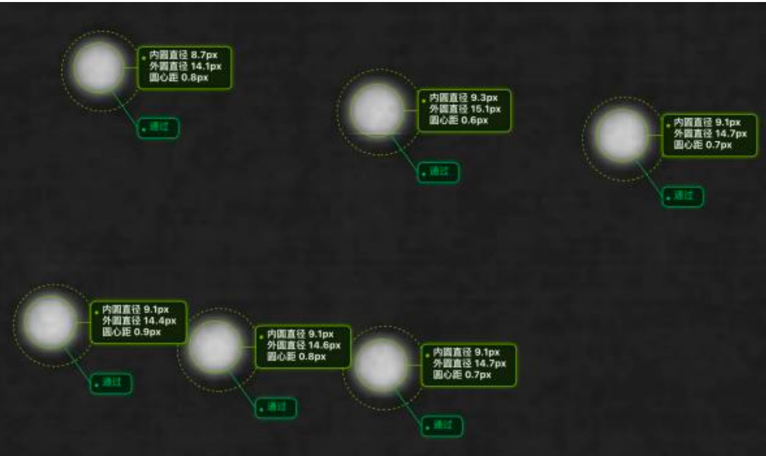
From too many holes to a verdict you can act on.
Coverage sampling can’t reach
Too many holes for sampling to cover, met with large-field imaging and parallel per-hole computation — you get per-hole results and a full-panel quality map instead of a sampled estimate.
Dimensional drift caught in time
Instead of finding drift too late, the system outputs diameter, roundness, position, and concentricity for every hole — supporting process tuning and anomaly tracing while there is still time to act.
Consistent burr and nick verdicts
Ambiguous burr and nick calls are handled by hole detection fused with geometric verdict models — less manual re-judgment and more consistent verdicts across inspectors and shifts.
Every number here comes with its method.
These are typical values, not guarantees. Each depends on optical configuration, field size, and sample condition, and is calibrated on your samples before it goes into the technical agreement.
| Metric | Typical value | Definition & calibration | Acceptance recommendation |
|---|---|---|---|
| Field size | 250–1000 mm | Single-shot imaging field for large-format panels; usable field depends on optical configuration and pixel size. | Derive from panel format and minimum measurable feature; confirm during validation. |
| Targets per panel | 5K–10M holes | Holes covered per panel at 100% inspection of dense arrays; actual count depends on hole density and panel size. | Confirm against your densest board on a representative sample. |
| Measurement repeatability | 1–3 μm | Dispersion (±3σ) of repeated measurements at the same position on the same sample; varies with objective magnification, pixel size, and surface condition. | GR&R-calibrated on your samples and written into the technical agreement. |
| Inspection throughput | 20K holes/s | Baseline for a single compute configuration; varies with field size, resolution, and compute, which is scalable. | Derive configuration from target takt; confirm during the pilot. |
Every published metric is explainable, calibratable, and verifiable — a method, not just a number. Typical values vary with optical configuration, field size, and sample condition; they are calibrated on your samples and written into the technical agreement.
Adopt in phases, with risk controlled at each step.
Software solution
Start hereDetection and metrology models, the inspection platform, and interfaces — validate offline before touching the line.
- Metrology and detection models
- Inspection platform
- Data and system interfaces
Integrated hardware-software unit
Algorithms packaged with an AI compute box and industrial integration for line-side deployment.
- Algorithms and AI compute box
- Industrial integration
- Line-side / inspection-station deployment
Standard equipment
Full machineA full machine with the AI inspection system and a closed data loop, for formal acceptance and multi-line replication.
- Full inspection machine
- AI inspection system
- Closed data loop
Output includes OK/NG verdicts, coordinates, size deviations, and defect classes; panel maps and heatmaps with traceable re-judgment; and reports and trends in CSV, image, or custom formats.
Questions procurement and engineering actually ask.
We already have AOI — do we still need this?
How many samples do you need to start?
Can we start small?
Send us 2–3 panels. Get back a feasibility conclusion.
Start a validation: send 2–3 representative panels — good parts plus known anomalies — and Insightek returns a feasibility conclusion and a metrology demo report.