Post-Dicing Inspection & Edge Quantification
Intercept bad dies at the post-dicing stage — before they consume downstream packaging materials, bonding hours, and whole-unit test cost.
Diced edges and sidewalls are the high-risk zone entering advanced packaging. Full-wafer inspection at the post-dicing stage detects edge anomalies, separates real defects from saw marks, and outputs position, size, and class — so high-risk dies are caught before they move on.
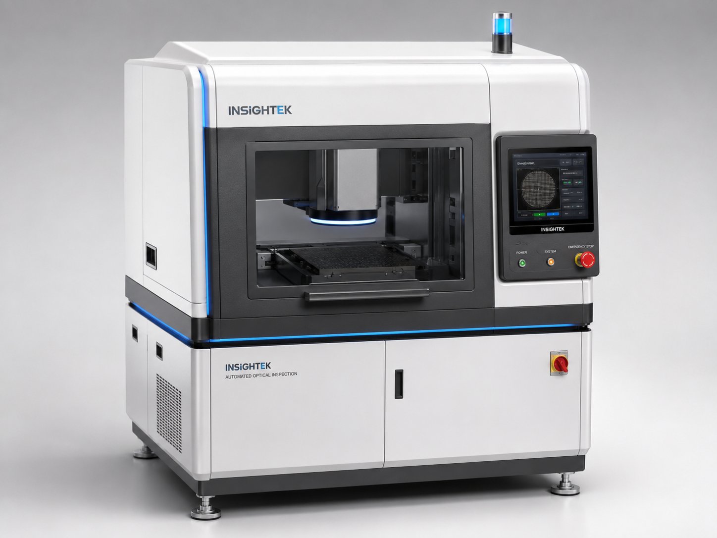
Three things that decide whether edge inspection actually holds up.
Large field, high resolution, high speed
High-speed micron-level stitching plus hardware-accelerated compute covers the full wafer at the resolution edge defects demand — and throughput scales with the compute you allocate.
AI that separates real defects from saw marks
Dedicated models trained on your samples distinguish real cracks, chipping, and particles from normal saw-cut texture — the confusion that drives most re-judgment load on diced edges.
All in-house, one owner closes the loop
Models, software, AI compute, and equipment are all self-developed. Accuracy, speed, and false-call issues never bounce between vendors — one owner is accountable for the result.
Edge defects that escape dicing get paid for in packaging.
The diced edge and sidewall are the high-risk zone entering advanced packaging — and a bad die that slips through does not stop costing until much later in the flow.
Edge and sidewall are the high-risk zone.
Cracks, chipping, and particles concentrate on the diced edge and sidewall — exactly the region that has to survive bonding and advanced packaging downstream.
Defects are tiny and easy to miss.
Cracks, chipping, and particles are small; low-coverage sampling and manual inspection are poor at catching this kind of local drift across a full wafer.
One escape multiplies its cost downstream.
As a general 1-10-100 rule of thumb, a defect caught at its own step costs 1, the next step 10, and at the customer 100. One bad die entering packaging wastes packaging materials, bonding hours, and whole-unit test cost.
Saw marks look like real defects.
Normal saw-cut texture is easily confused with genuine damage, inflating re-judgment load and eroding trust in whatever verdict the line produces.
From your samples to a line-side loop, in five steps.
Each step has a defined deliverable, and each step tells you what both sides do — so you always know what you receive before committing to the next stage.
- 01
Sample & process review
You provide representative diced wafers or dies and your target metrics; Insightek assesses feasibility against your dicing process. You receive a feasibility conclusion.
- 02
Imaging & algorithm validation
Insightek selects the optics and imaging mode for edge and sidewall defects and validates the detection models on your samples. You receive a detection and quantification demo report.
- 03
Inspection items & thresholds
Verdict thresholds and acceptance criteria for cracks, chipping, notches, and particles are agreed on a mutually confirmed sample set. You receive a verdict scheme plus acceptance criteria.
- 04
Line-side integration & data output
Interfaces are hooked up, pilot runs confirm takt, and defect position and size data flows to your systems. You receive an integration validation report.
- 05
Acceptance, replication & iteration
Formal acceptance, replication across lines, and model iteration per your re-judgment rules to keep reducing overkill and escapes. You receive an acceptance report plus a maintenance plan.
To prepare, gather good, defect, borderline, and re-judgment samples, your target metrics (accuracy, escape/overkill, takt), your inspection point and interfaces (PLC/MES/SPC/SECS-GEM or report formats), and your acceptance rules.
The edge and sidewall defects that matter after dicing.
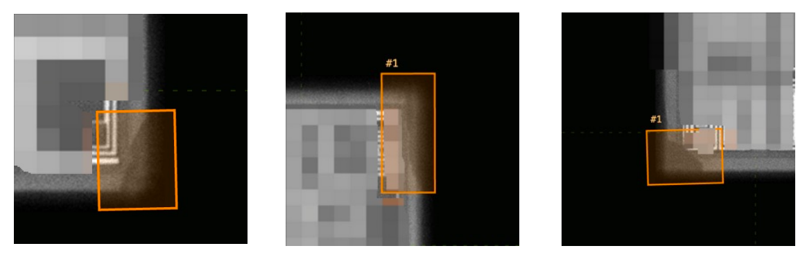
On a full wafer, the system finds dicing-edge anomalies, draws bounding boxes, and outputs position, size, and class — with AI separating real defects from saw marks.
Low-k sidewall / hairline cracks
The historically hard-to-detect class: fine cracks on sidewalls, including low-k material stacks.
- Targets sidewall and hairline cracks that manual and low-coverage inspection routinely miss
- Detectability depends on imaging mode and the dicing process — verified with defect samples
- Covers low-k and brittle materials
Chipping / notches
Edge chipping and notches, detected and measured rather than only flagged.
- Quantified size output for each chipping or notch event
- Bounding box plus position, size, and class per defect
- Consistent measurement across the full wafer
Edge burrs / particles
Burrs and particles along the diced edge, screened across the whole wafer rather than by spot check.
- Full-wafer coverage via high-speed micron stitching
- Distinguishes particles and burrs from normal saw-cut texture
- Position and size output for traceability
Minute surface anomalies
Small surface anomalies on the die, held to a detection limit set on your samples.
- Detection limit calibrated on your defect and borderline samples
- Smallest stably detectable size depends on optical resolution and contrast
- Criteria confirmed on a mutually agreed sample set
Scope & boundaries
What this covers, and honestly where results depend on conditions.
- Applies to diced wafers and dies, including low-k and brittle materials
- Sidewall-crack detection depends on imaging mode and dicing process, and is verified with defect samples
- Real-vs-false discrimination is trained on your samples and iterated per your re-judgment rules
From a floor problem to a quantified verdict.
Escapes caught before packaging
Post-dicing edge defects that would otherwise escape downstream are intercepted by full-wafer inspection at the post-dicing stage — high-risk dies are caught early, before they consume packaging cost.
Tiny defects turned into numbers
Cracks, chipping, and particles are tiny. Dedicated defect models plus edge quantification output each defect's position, size, and class — not just a pass/fail flag.
Less re-judgment, with traceability
Saw marks confused with real defects are the usual re-judgment burden. Verdicts built from sample training plus your re-judgment rules cut that load and support traceability.
Typical values — with how each one is defined and calibrated.
These are typical values. Actual figures vary with optical configuration, field size, and sample condition, and are calibrated on your samples and written into the technical agreement.
| Metric | Typical value | Definition & calibration | Acceptance recommendation |
|---|---|---|---|
| Target | Wafer / die (incl. low-k) | Diced wafers and dies, including low-k material stacks. Detection capability is the smallest stably detectable defect, depending on optical resolution and contrast. | Calibrate detection capability with your defect and borderline samples; set the detection-limit, overkill, and escape criteria on a mutually confirmed sample set. |
| Coverage | Full wafer | Full-wafer coverage achieved by high-speed micron-level stitching across the diced surface and edges. | Confirm the inspected region and stitching field against your wafer and dicing layout during the pilot. |
| Speed | < 0.5 s / cycle | Stitching plus inspection per cycle, quoted as a baseline for a single compute configuration; varies with field size, resolution, and compute, which is scalable. | Derive the configuration from your target takt and confirm speed during the pilot. |
| Output | Position + size | Defect position and quantified size, with bounding boxes and class; AI verdicts separate real defects from saw marks. Verdict consistency is the repeat-consistency of AI verdicts on the same batch. | Accept verdict consistency via a blind-test sample set against human re-judgment; models improve as new samples are added. |
Metrics are typical values and vary with optical configuration, field size, and sample condition. Every value is calibrated on your samples and written into the technical agreement — the method is disclosed, not just the number.
Adopt in phases, with the risk controlled at each step.
Software solution
Start hereDetection models plus the inspection platform and interfaces, for teams that already have imaging or want to start with offline validation.
- Defect models and the inspection/quantification platform
- Data and reporting interfaces
- A low-commitment entry point via software and offline validation
Integrated HW-SW unit
Algorithms plus an AI compute box and industrial integration, delivered as a combined unit for line-side deployment.
- Detection algorithms packaged with an AI compute box
- Industrial integration for the inspection station
- A step up once offline validation is confirmed
Standard equipment
Full deliveryA full machine with the AI inspection system and a closed data loop, for standardized post-dicing inspection.
- Complete machine plus AI inspection system
- Closed data loop for wafer maps and traceable re-judgment
- For multi-line replication once the scheme is accepted
Output includes OK/NG verdicts, coordinates, size deviations, and defect classes, presented as wafer maps and heatmaps with traceable re-judgment, plus reports and trends in CSV or image form.
Questions engineering and procurement actually ask.
We already have AOI — do we still need this?
How many samples do you need to start?
Can we start small?
Start a validation on your own diced samples.
Send diced samples with known cracks or chipping plus good references. Insightek returns a detection validation and quantification demo report — measured on your material, not a generic spec sheet.